
At the Hot Chips 2026 international high-end chip technology conference, Samsung and SK hynix laid out their next-generation HBM4 evolution roadmaps. Unlike previous iterations that centered on raising DRAM speed and increasing stack layer counts, the new HBM4 generation is defined by three innovation fronts: Base Die logic process upgrades, hybrid-bonding 3D stacking, and EMIB heterogeneous packaging. The industry’s long-standing HBM iteration playbook is being rewritten.
The driving force is direct: AI large language model training and inference demand continues to surge, and the performance bottleneck of AI compute chips has shifted from computing units to memory bandwidth. In ultra-high-bandwidth scenarios, simply increasing DRAM speed introduces signal crosstalk, soaring power consumption, and timing skew. Two-dimensional planar optimization can no longer support the massive compute loads, making HBM the critical constraint on high-end AI hardware advancement.
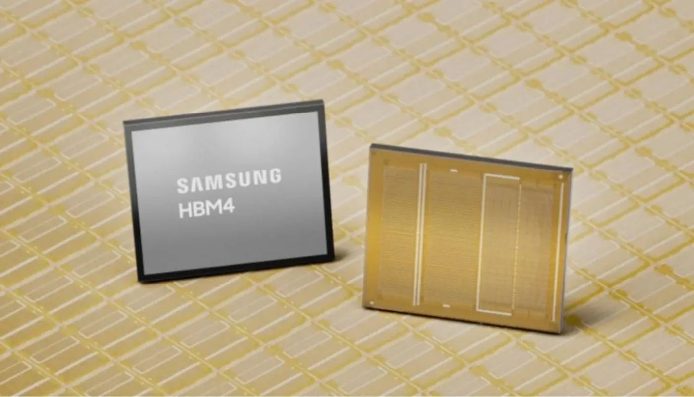
The two memory giants are clearly diverging in their technical approaches. Samsung disclosed that its HBM4/HBM4E Base Die adopts a 4nm logic process, with pin data rates up to 11.7Gbps and per-stack bandwidth reaching 3.3TB/s, while also pushing some memory control logic down to the Base Die. SK hynix, by contrast, is cooperating with TSMC on a 12nm logic process, placing greater emphasis on production stability and compatibility with ultra-high stack architectures. These two routes mean HBM4’s internal logic architecture is no longer uniform, adding new complexity to supply chain adaptation and chip design iteration.
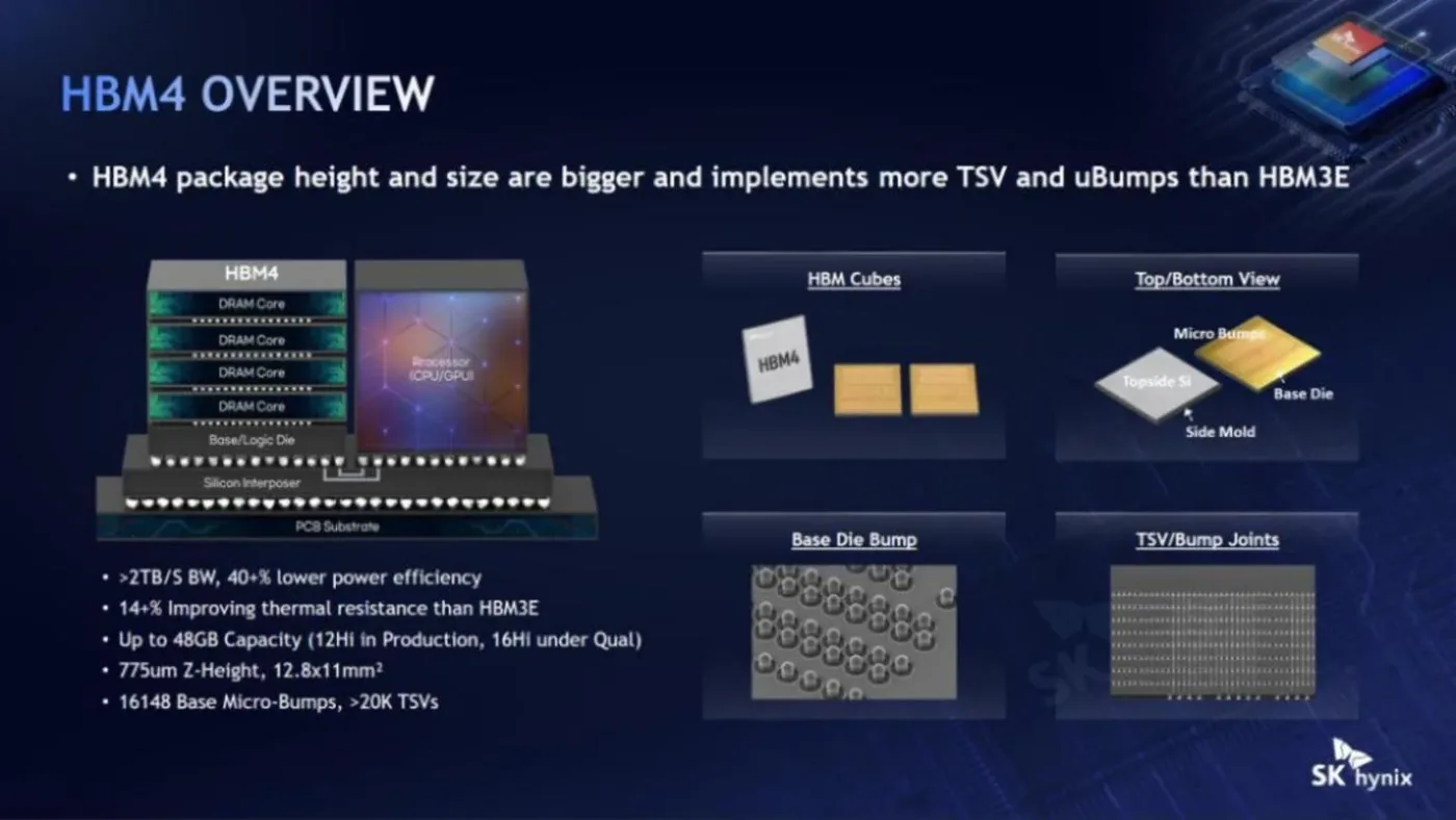
Shifting the Base Die to a logic process brings multiple benefits: higher transistor density improves signal integrity and power efficiency, while providing the physical headroom for doubled I/O width and near-memory computing, making HBM far more than a passive data container. But the cost is equally significant. HBM is no longer a product that memory makers can fully deliver in a closed loop. Logic foundry capacity, IP design capability, and cross-process co-simulation are now production constraints, stretching design verification cycles and multiplying supply chain complexity.

Packaging routes are also diversifying. TSMC’s CoWoS is no longer the only solution; hybrid packaging approaches are entering the picture, and internal stacking bonding is moving toward hybrid-bonding 3D. The common direction is clear: HBM is transforming from a single memory component into an integrated “memory + logic + packaging + IP + EDA” system. The technical barrier now extends from DRAM manufacturing into the entire semiconductor supply chain.
For downstream AI computing platforms, HBM evolution directly affects the supply and cost of high-end GPUs. Higher bandwidth eases the memory-wall pressure in large model training and inference, but rising supply chain complexity and costs will inevitably pass through to compute pricing. Finding a balance among high bandwidth, high cost, and supply stability is a practical issue for every computing platform operator — and a key variable that StarWar Cloud continues to monitor in its GPU compute capacity planning.